Difference between revisions of "Fitlet3: COM + GPIO connector pinout"
From fit-PC wiki
| Line 121: | Line 121: | ||
* The GPIO feature needs the newest FPGA version. | * The GPIO feature needs the newest FPGA version. | ||
| + | '''GPIO access explanations:''' | ||
| − | Actual connector's pinout: | + | ''1. fitlet3 has 2 GPI and 2 GPO.'' |
| + | GPI: Pins 4 and 5 | ||
| + | GPO: Pins 2 and 3 | ||
| + | [[File:Terminal Block Connector.jpg|thumbnail|center]] | ||
| + | Actual connector's pinout: | ||
| + | [[File:GPIO_COM_CONNECTOR.png|thumbnail|center]] | ||
| + | ''2. The GPIOs are controlled by the PCA9555 SMBUS I/O expander: https://www.ti.com/lit/gpn/pca9555'' | ||
| + | It is located on the SMBUS address 0x20 in 7-bit format or 0x40 in 8-bit format. | ||
| + | The GPIO map: | ||
| + | [[File:IO Expander.jpg|thumbnail|center]] | ||
| + | ''3. The GPIOs are controlled through SMBUS I/O expander registers: Input Port 1 (Command Byte: 0x01) and Output Port 1 (Command Byte: 0x03)'' | ||
| − | + | To control GPO0 - write 0 or 1 to SMBUS address 0x20, byte 0x03, bit 0x05 | |
| − | + | To control GPO1 - write 0 or 1 to SMBUS address 0x20, byte 0x03, bit 0x06 | |
| − | + | To read GPI0 - read from SMBUS address 0x20, byte 0x01, bit 0x07 | |
| + | To read GPI1 - read from SMBUS address 0x20, byte 0x01, bit 0x01 | ||
Revision as of 12:47, 25 June 2023
General COM + GPIO connector pinout
| Pin Number | RS232+GPIO | RS485 Half duplex +GPIO | RS485 Full Duplex +GPIO |
|---|---|---|---|
| 1 | Power In | Power In | Power In |
| 2 | GPO (output) | GPO (output) | GPO (output) |
| 3 | GPO (output) | GPO (output) | GPO (output) |
| 4 | GPI (Input) | GPI (Input) | GPI (Input) |
| 5 | GPI (Input) | GPI (Input) | GPI (Input) |
| 6 | TXD | Data- | TX- |
| 7 | RXD | RX+ | |
| 8 | CTS | RX- | |
| 9 | RTS | Data+ | TX+ |
| 10 | GND | GND | GND |
The COM port connector contains: Serial communication (RS232, RS485 Half duplex, and RS485 Full duplex). GPIO (2 Input and 2 Output).
Serial communication pinout:
| Pin Number | RS232 | RS485 Half duplex | RS485 Full Duplex |
|---|---|---|---|
| 6 | TX | TXN/RXN | TXN |
| 7 | RX | - | RXP |
| 8 | CTS# | - | RXN |
| 9 | RTS# | TXP/RXP | TXP |
GPIO pinout:
| Pin Number | GPIO |
|---|---|
| 1 | VCC |
| 2 | GPO 0 |
| 3 | GPO 1 |
| 4 | GPI 0 |
| 5 | GPI 1 |
| 10 | GND |
- The GPIO requires an external VCC to function. (up to 24V)
- The GPIO feature needs the newest FPGA version.
GPIO access explanations:
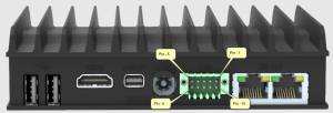
1. fitlet3 has 2 GPI and 2 GPO.
   GPI: Pins 4 and 5
   GPO: Pins 2 and 3
Actual connector's pinout:
2. The GPIOs are controlled by the PCA9555 SMBUS I/O expander: https://www.ti.com/lit/gpn/pca9555
   It is located on the SMBUS address 0x20 in 7-bit format or 0x40 in 8-bit format.
   The GPIO map:
3. The GPIOs are controlled through SMBUS I/O expander registers: Input Port 1 (Command Byte: 0x01) and Output Port 1 (Command Byte: 0x03)
   To control GPO0 - write 0 or 1 to SMBUS address 0x20, byte 0x03, bit 0x05
   To control GPO1 - write 0 or 1 to SMBUS address 0x20, byte 0x03, bit 0x06
   To read GPI0 - read from SMBUS address 0x20, byte 0x01, bit 0x07
   To read GPI1 - read from SMBUS address 0x20, byte 0x01, bit 0x01


